
Most of the theory we discussed earlier in the book involved the physics of gas lasers, where the electron energy states in the light-amplifying medium are discrete energy states of relatively isolated atoms. The electron energy states in a solid semiconductor crystal are very different. The electron energy states in a semiconductor form bands, which are large sets of energy states closely spaced in energy. The bands of energy states in a semiconductor are separated by band gaps, which are energy ranges in which there are no electron states. We are interested in two bands of electron states: the lower-energy valence band and the upper-energy conduction band, which are separated by a band gap, as diagrammed below.
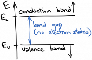
This sort of diagram is called a band-edge diagram, as we only show the edges of the bands. The energy of the bottom edge of the conduction band is called $latex E_C$, and the energy of the top edge of the valence band is called $latex E_V$. The difference $latex E_C – E_V$ is the width of the band gap, $latex E_G$.
There are broadly two ways that we can understand how these bands are formed. The first is to imagine isolated atoms, with their discrete energy levels, being gradually brought together. As atoms move into proximity to one another, their electron energy states split into upper and lower energy states due to their interactions. Repeat this for the roughly $latex 10^{26}$ atoms in a macroscopic sample of the material, and the discrete states transform into bands.
The second way to understand bands is to imagine a free electron in space. Similar to an electromagnetic wave, in free space the allowed electron states are plane waves. Now, let’s gradually ‘turn on’ the periodic electrostatic potential of the atomic nuclei in the semiconductor. As our electron plane wave encounters these potential barriers, it will partly reflect and partly transmit. For certain electron frequencies (energies), destructive interference will occur for the transmitted waves, meaning that the electron wave can’t travel through the material at that energy. Thus, the band gap.
A more complex depiction of the electron energy states in a semiconductor is the bandstructure, which plots each electron state’s energy (on the y-axis) against its momentum (on the x-axis). Here is a link to a nice diagram of the bandstructure of GaAs:
http://backreaction.blogspot.com/2007/12/band-structure-of-gallium-arsenide.html
Let’s contrast this with the bandstructure of Si:
http://www.iue.tuwien.ac.at/phd/wessner/node31.html
You’ll notice that in GaAs, the minimum energy of the conduction band and the maximum energy of the valence band both occur at the $latex \Gamma$ point – in other words, those states have the same momentum. This is called a direct band gap. On the other hand, in Si the minimum energy of the conduction band is misaligned with the maximum of the valence band; this is an indirect band gap. This has an impact on light emission, as we’ll discuss later.
You must be logged in to post a comment.