
Research
Dr. Klein’s group carries out theoretical modeling and numerical simulation of the internal physics of electronic, optoelectronic, and optical devices in order to deepen our fundamental understanding of their operation and improve their design. The simulations are performed using a wide array of computational resources, including a 44 node Beowulf-class cluster.
GaN-based light emitting diodes and lasers
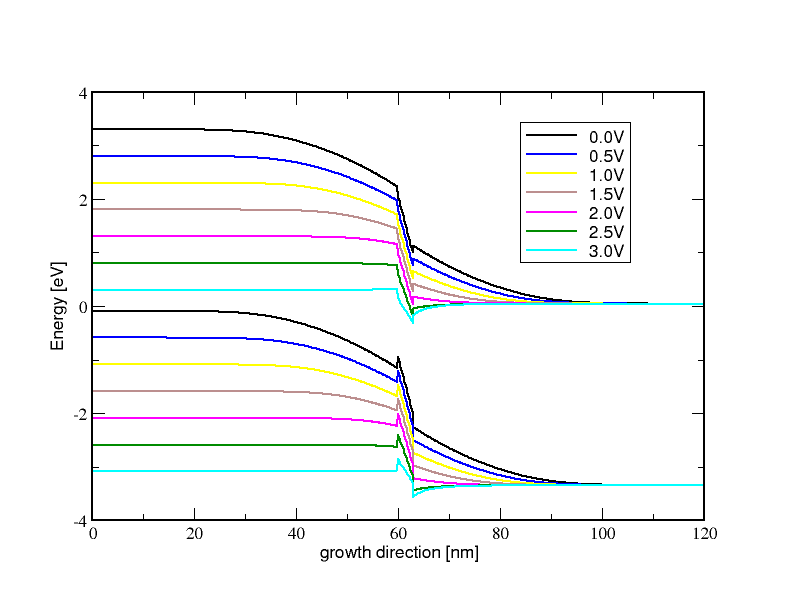 Due to their large bandgap energies, the InGaN and AlGaN material systems are used extensively to produce green, blue, violet, and UV LEDs and lasers, for applications ranging from telecommunications to high-density data storage to room lighting. However, these materials also present unique challenges. For example, strong piezoelectric and spontaneous polarization fields are found in these hexagonal crystal lattices when they’re grown on the commonly used c-plane. These fields bend the band edge diagram, as shown in the figure to the right, and drive bound electrons and holes apart within the quantum wells of the system, thus reducing the matrix element for optical recombination. We solve the nonlinear Poisson equation in the presence of the electron and hole populations and the polarization charges to accurately predict and design the band edge profile. The band edge profile provides the input to our k.p solver for the electron and hole bound states in the quantum wells.
In our research, we efficiently couple this microscopic model of the active region to models of bulk carrier transport and heating, in order to provide fast and accurate first-order models for rapid device design and elucidation of experimental results. We focus particularly on novel device designs, such as nanowire and photonic crystal LEDs and lasers, and novel substrates (such as ZnO). This work is done in collaboration with the experimental group of Dr. Ian Ferguson at Georgia Tech in Atlanta, and Dr. Norman Sanford at NIST.
GaN nanowire field effect transistors
In collaboration with Dr. Norman Sanford and Dr. Kris Bertness of the National Institute of Standards and Technology in Boulder, Colorado, we investigate GaN nanowire field effect transistors prepared with a source and drain contact on either end, and a gate contact wrapped around the waist. We numerically calculate pinchoff voltages and resistance as a function of gate voltage, to assist in the experimental characterization of the wire doping levels and mobilities.
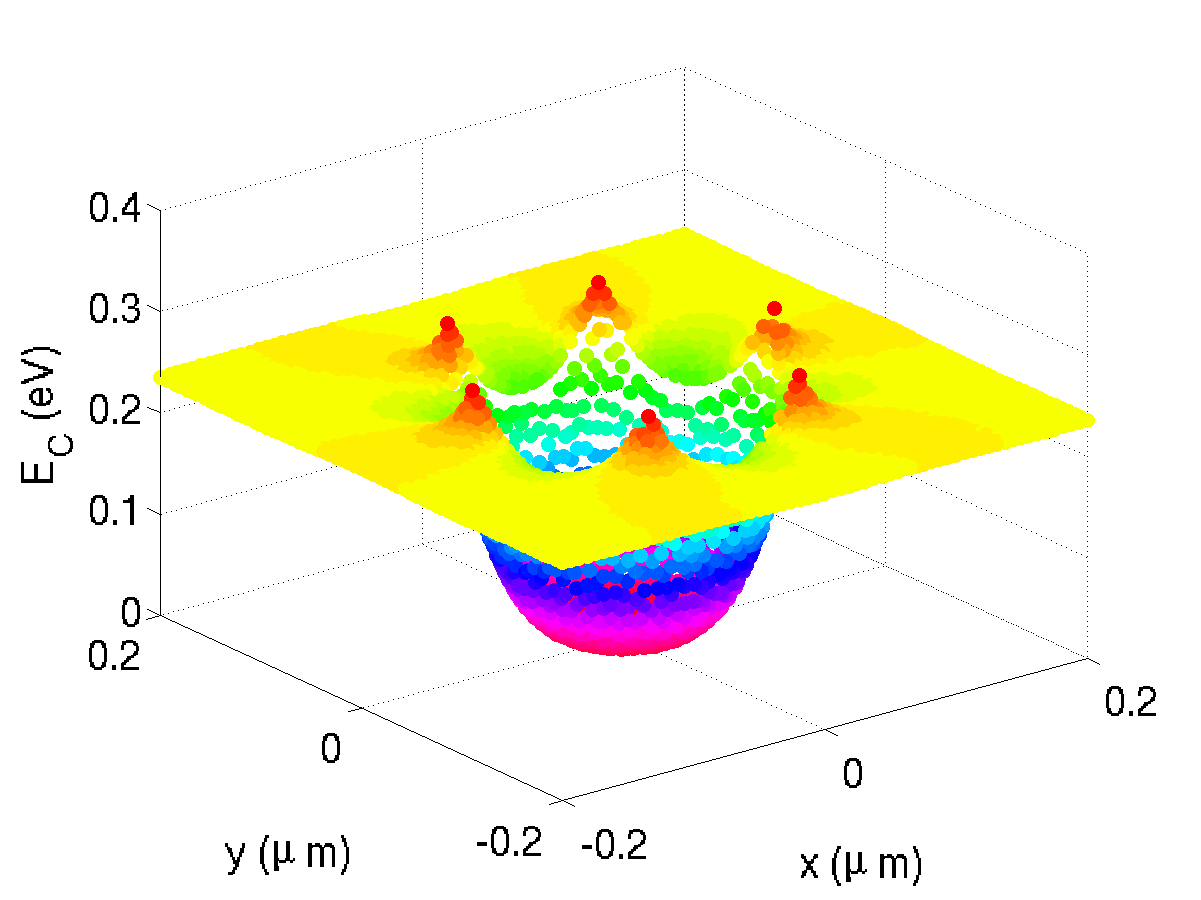
In addition, we investigate surface band-bending due to surface acceptor states. On the left is shown the conduction band edge diagram for a cross-section of a hexagonal nanowire, showing the surface band bending phenomenon.
Our ongoing research is to analyze the dynamic response of these nanowire devices to light pulses of sufficiently short wavelength to generate significant electron and hole densities, which temporarily compensates for the band bending effect.
Robust photonic crystal waveguide coupler design
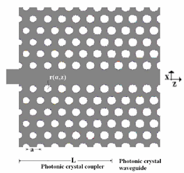 Photonic crystal waveguides can make sharp turns without suffering optical loss, and offer unprecedented control over the dispersion of waveguide modes, including the possibility of ‘slow light’: optical modes with very slow group velocities. This is of interest for all-optical signal processing, amongst other applications. However, when coupling light into a slow-light waveguide directly from a conventional ridge waveguide, most of the radiation is reflected due to the large impedance mismatch. Therefore, is it necessary to use a coupler to enhance the transmission of light from a conventional waveguide to a slow-light waveguide, as shown on the right. Using our Fourier modal method code, we have calculated optimum coupler designs.
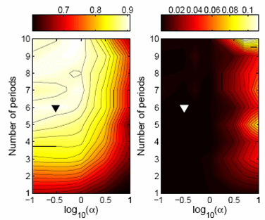 In collaboration with Dr. Janet Allen of the Systems Realization Lab at Georgia Tech, we also explored robust design concepts for the photonic crystal waveguide coupler. During the fabrication process, unavoidable random fluctuations will occur in the diameter of the etched holes. Due to this, the optimum solution may not be possible to fabricate in practice. Therefore, we model the random fluctuations in hole diameter in each period of the coupler, and calculate a more robust design that combines high transmission with low variation in the transmission due to random hole diameter fluctuations. Shown to the left are the calculated transmission (left) and the standard deviation of the transmission (right) as a function of a coupler profile parameter, and a more robust design is indicated. Since the impact of fluctuations increases with overall coupler length, the more robust design is shorter than an optimum design.
Photonic crystal vertical-cavity surface-emitting lasers (VCSELs)
 As shown on the left, photonic crystal VCSELs incorporate 2D photonic crystal defect cavities into the upper distributed Bragg reflector (DBR) mirror by etching holes into the top surface of the device. This is done primarily to increase the modal discrimination and prevent multimode lasing at high injection currents, by exploiting the analogy to endlessly single-mode photonic crystal fibers. Due to the large size of the structure and the nonseparable nature of the geometry, this presents a challenging design and simulation problem. We have developed a Fourier modal method code that finds the complete set of propagating and evanescent modes in each vertical layer of the device, then couples modes between layers using a scattering matrix.
![]() The presence of a defect cavity in the photonic crystal layers introduces a large number of guided modes in the core region. On the right is shown the calculated normal-incidence transmission through a single layer of defect cavity-free photonic crystal slab (solid line), along with the calculated transmission through the same slab layer with a single hole removed to form an in-plane defect cavity (dotted line). The additional fluctuations in the transmission near the resonance are due to guided modes in the defect. The fundamental mode has a much sharper resonance than the higher-order modes, which lose radiation to the boundaries. Research is ongoing to completely analyze the modal discrimination properties of photonic crystal DBRs.
The presence of a defect cavity in the photonic crystal layers introduces a large number of guided modes in the core region. On the right is shown the calculated normal-incidence transmission through a single layer of defect cavity-free photonic crystal slab (solid line), along with the calculated transmission through the same slab layer with a single hole removed to form an in-plane defect cavity (dotted line). The additional fluctuations in the transmission near the resonance are due to guided modes in the defect. The fundamental mode has a much sharper resonance than the higher-order modes, which lose radiation to the boundaries. Research is ongoing to completely analyze the modal discrimination properties of photonic crystal DBRs.
In addition, the impact of a photonic crystal DBR on the current flow through the VCSEL is of great importance. The free surfaces at the hole edges are likely to contain many defect states, and provide an unwanted dark recombination path for carriers in the device. To model this, we use our 3d bulk carrier transport simulator.
Antiguided VCSELs and arrays
 Antiguided VCSELs are designed so that the effective refractive index of the laser cavity is less than that of the cladding in the in-plane direction. Although this increases the optical loss of all modes, the higher-order modes suffer a much greater penalty (especially in their overlap with the gain region), and therefore modal discrimination is enhanced. If many antiguided VCSELs are placed adjacent to one another, they may couple and form a coherent array, analogous to an antenna array. This can be exploited to achieve very high single-mode output powers, in excess of a watt. However, it is clear that the traditional passive-cavity mode approximation is not valid for these structures, since they are gain-guided: the gain is the only reason the mode is bound to the cavity at all. Therefore, we employ an active-cavity mode solver based on the electromagnetic Green’s function of layered structures, combined with the method of moments, to solve the integral equation representing the self-consistency of the lasing mode above threshold. In this way we can accurately predict both the resonant frequencies and the gain required to lase for high-power VCSEL arrays.
Lasing in metal-clad micropost cavities
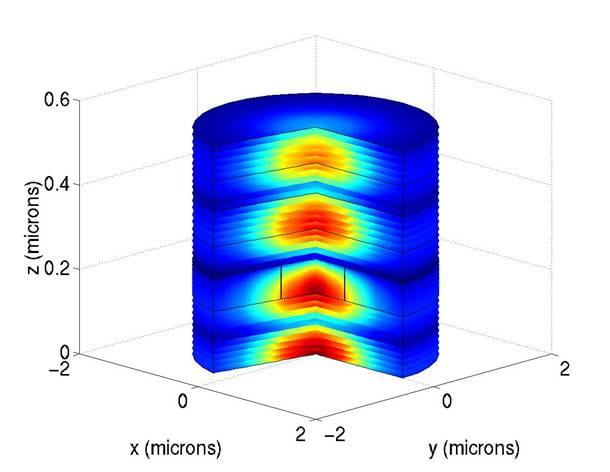
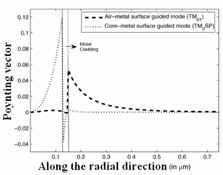 Metal surfaces in optical devices introduce a special class of optical modes known as ‘surface plasmon modes’ (a plasmon is a quantum of the collective oscillations of the free electrons in a metal). These modes cling to the metal surface, and are effectively evanescent in the direction normal to the surface, but can propagate along the surface. Due to their partly-evanescent nature, it is possible to confine these modes to subwavelength dimensions in the direction normal to the metal surface, which is otherwise impossible to accomplish for a propagating mode. This is an attractive property from the perspective of miniaturization of optical components. However, these modes suffer a significant penalty in the form of large optical losses due to free-carrier absorption. In this work, we examine whether it is possible to exploit surface plasmon modes to lase in a subwavelength-scale cylindrical micropost coated in metal. The calculated surface plasmon modes (both interior and exterior) of the metal-clad micropost are plotted at left. It is found that for a wavelength of one micron, the losses exceeded the available gain from a bulk semiconductor gain medium. A gain medium with a larger material gain, as well as operation at longer wavelengths, would be more successful.
The mission of the Computational Electronics Group is to provide theoretical and simulation-assisted physical analysis and design of optical and electronic devices. We achieve fast, practical solutions tailored to the needs of our experimental partners. We welcome discussions with potential collaborators, please feel free to contact us!
