
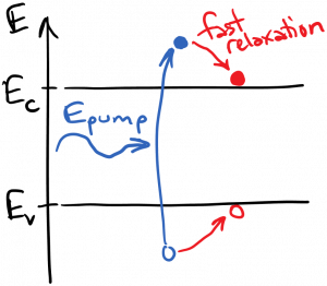
We can invert the band-edge states in a semiconductor by optically pumping with photons whose energy is significantly greater than the band gap energy. This resembles a four-level pumping scheme. As we’ve discussed, electrons and holes generated far from the band edges will rapidly relax to band-edge states, which is desirable for a four-level scheme. This is diagrammed below.
For most applications, electrical pumping is preferable to optical pumping. Electrical pumping is accomplished by placing the optical gain region (the semiconductor we wish to invert) in the middle of a p-n junction diode. This is diagrammed below. When forward biased, the diode will inject electrons from the n-side into the gain region, and holes from the p-side into the gain region.

It can be shown that the energy difference between the quasi-Fermi levels in the gain region is approximately equal to the electron charge times the voltage applied across the diode $latex V_A$, or
$latex \displaystyle F_n – F_p \equiv q V_A$
This means that, to achieve inversion, we must have $latex q V_A > E_G$, where $latex E_G$ is the band gap energy of the gain region.
It is not necessary that the gain region be composed of the same type of semiconductor as the surrounding p-n junction. In fact, it is preferable to choose a smaller band gap material for the gain region. This traps electrons and holes in the gain region, and increases the inversion. As you can see from the equation above, a smaller band gap also reduces the applied voltage required for inversion. A semiconductor laser containing multiple semiconductor materials of differing band gap energies is called a heterojunction diode laser. All practical laser diodes are heterojunctions.
You must be logged in to post a comment.