
Similar to the optical transitions we studied earlier, in semiconductors electrons can make transitions between two energy states and create or destroy photons in the process. In particular, transitions between the conduction band and the valence band (‘interband transitions’) are optically active, as the lower conduction band generally consists of s-like states while the upper valence band consists of p-like states. Spontaneous emission, absorption, and stimulated emission can all take place between conduction band states and valence band states.
Let’s consider absorption first. As before, the ingredients for optical absorption are an incoming photon, a valence band energy state occupied by an electron, and an empty conduction band energy state. In equilibrium, the valence band is mostly full and the conduction band is mostly empty, so these conditions are easily met. Recall that optical absorption between two states in an atom only occurred for a narrow spectrum of photon energies (the linewidth of the transition). By contrast, optical absorption in a semiconductor can occur over a wide range of photon energies, as long as the photon energy is greater than or equal to the band gap energy. This is diagrammed below.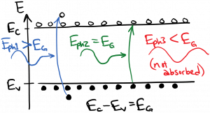
Since the absorption process creates an electron in the conduction band and a hole in the valence band, it is also called optical generation. Note that electrons created at energies higher than the band edge will quickly relax to the lowest conduction band energy states (band edge states) by releasing phonons. Similarly, holes created deep in the valence band will ‘float up’ to the valence band edge.
Moving on to spontaneous emission, this process requires a conduction band energy state occupied by an electron and an empty valence band energy state (we can shorten this to say ‘requires an electron and a hole’, since ‘electron’ generally refers to an electron in the conduction band). This is the opposite of the common situation in equilibrium, but at a finite temperature there will be a small number of full states in the conduction band and empty states in the valence band. Also, electrons and holes can be created via optical absorption and other pumping mechanisms we’ll describe later. As with absorption, the spontaneous emission process is possible for a wide range of photon energies above the band gap; but in practice, the conduction band states most likely to be full are those lowest in energy, just as the valence band states most likely to be empty are those highest in energy. Therefore, the spontaneous emission observed from a semiconductor sample is most likely to have a photon energy nearly equal to the band gap energy. This is diagrammed below.
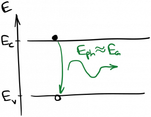
Since the spontaneous emission process ‘destroys’ an electron and a hole, it is also called spontaneous optical recombination.
At this point we can understand why ordinary silicon is not useful for light emission. As we saw, silicon has an indirect bandgap. That means that the lowest energy states in the conduction band have a different momentum than the highest energy states in the valence band. Unfortunately, those are the states that are most likely to be occupied by an electron and a hole, respectively. The spontaneous emission process must conserve both energy and momentum, but photons carry very little momentum (not zero!). Therefore, an electron at the ‘bottom’ of the conduction band is unable to recombine with a hole at the ‘top’ of the valence band via spontaneous photon emission, because that would violate conservation of momentum: the electron would have to undergo a significant momentum change, and the photon is unable to carry away enough momentum. The same logic also prevents stimulated emission in indirect band gap semiconductors.
Finally we have stimulated emission, the most important process for laser operation. As before, this process requires an incoming photon, an electron, and a hole. It produces a copy of the incoming photon. As with spontaneous emission, we expect that in most cases the stimulated emission will occur primarily between band-edge states, as these states are most likely to be occupied with electrons and holes. Thus, semiconductor optical amplifiers generally amplify light whose photon energy is approximately equal to the band gap energy of the semiconductor gain medium. The stimulated emission process is diagrammed below.
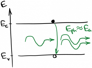
Since the stimulated emission process ‘destroys’ an electron and a hole, it is also called stimulated optical recombination. In order to make stimulated emission the dominant optical process, we need to achieve population inversion. This will be discussed in the next section.
You must be logged in to post a comment.