
A diode is an electronic device that only allows significant current flow in one direction. Our interest is to use a diode as a tool for injecting electrons and holes into a semiconductor gain medium, thus inverting it. Let’s understand a bit about how p-n junction diodes work.
A p-n junction diode is composed a semiconductor which has two adjacent regions. One region is doped with donor dopants, the other is doped with acceptor dopants. As a result, one region has an excess of electrons (the n-side), while the other has an excess of holes (the p-side). Electrons will diffuse from the n-side to the p-side, and holes will diffuse from the p-side to the n-side, but this diffusion process leaves behind the charged (ionized) dopant atoms, whose locations remain fixed in the crystal. Therefore, the region near the boundary between the p-side and the n-side is depleted of electrons and holes (which have diffused to the other side), and there exists a space charge in that depletion region. This is diagrammed below.
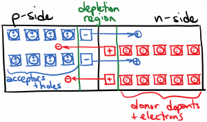
The space charge creates a built-in electric field which points from the n-side towards the p-side in the depletion region. In equilibrium, there exists a balance. Further diffusion is prevented by the built-in electric field, which pushes electrons and holes back towards the n-side and p-side, respectively. If we apply a voltage across the device, we create an external electric field. If the external electric field is aligned with the built-in electric field (‘reverse bias’), the built-in field is reinforced, and electrons and holes will be confined to the n-side and p-side, respectively. If the external electric field has the opposite orientation as the built-in electric field (‘forward bias’), the built-in field is partly or wholly cancelled, and electrons and holes will diffuse across the junction, creating a large current. This is why current only flows one way in a p-n junction diode. This is diagrammed below.

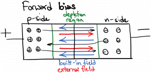
Our interest is less in the electronic properties of the device. We want to invert a semiconductor, which requires the injection of both electrons and holes. By placing the optically amplifying region in the depletion region and forward-biasing the diode, we will inject electrons from the n-side and holes from the p-side.
You must be logged in to post a comment.